
What an FPGA is
FPGA means field-programmable gate array: an integrated circuit with configurable logic and interconnect. A design configures hardware behaviour rather than simply supplying instructions to a fixed processor. Device resources are finite; an FPGA cannot implement an unlimited or arbitrary circuit without capacity, timing and interface constraints.
Architecture and comparison
Logic resources implement functions and state; routing connects them. Depending on the family, dedicated memory, DSP blocks, transceivers and processor subsystems complement the programmable fabric. An MCU executes software on a fixed processor architecture; many also include hardware peripherals, accelerators and multiple cores. An FPGA can implement parallel pipelines, but it is not automatically faster or more efficient for every workload. A fixed ASIC can offer better efficiency for a specific high-volume task, at the cost of a different development and manufacturing commitment.
Some SoC FPGAs combine a processor capable of running Linux with programmable logic. Linux runs on the suitable processor subsystem, not directly on logic gates without a processor. Verify memory, board support and toolchain availability for the selected device.
Development workflow
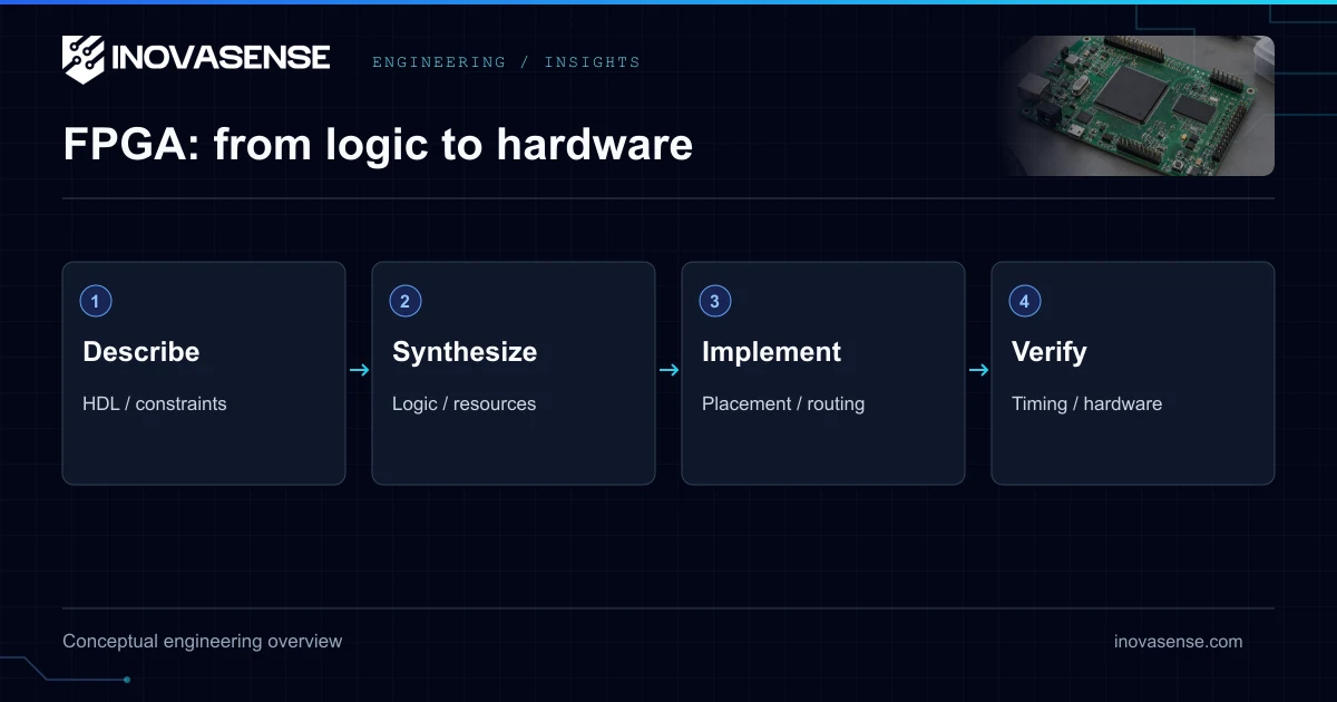
- Define interfaces, throughput, latency, clocks and reset behaviour.
- Design RTL or use a supported higher-level synthesis workflow.
- Simulate normal operation and failure cases before board testing.
- Synthesize, place and route; check timing constraints and clock-domain crossings.
- Verify the configured hardware on the target board.
- Version the bitstream, source, constraints, tools and test evidence.
Meeting timing requires correct constraints and verified design assumptions. Deterministic processing latency is an architectural result to demonstrate, not a guarantee provided by the FPGA name.
Cost, power and security
Budget depends on family, package, quantity, IP licences, tools, board complexity and verification effort. Use a current supplier quote instead of a universal device-price table. Estimate static and dynamic power with vendor tools, then measure representative operating modes; clocks, switching activity, memory and transceivers matter.
Authentication and encryption capabilities vary by family and configuration. Authentication protects against unauthorised configuration; encryption can protect bitstream confidentiality. Plan key handling, debug policy, update recovery and supported anti-rollback controls. Reprogrammability makes some field changes possible but does not itself prove security or legal conformity.
CRA and technology choices
CRA requirements are outcome-oriented and technology-neutral, based on the product’s cybersecurity risk assessment and applicability. Secure boot, a hardware root of trust, TPM, TrustZone and wireless OTA can be appropriate engineering controls; they are not universal legal mandates for every product. Document why the chosen controls satisfy the applicable requirements rather than equating one architecture with compliance.
Applicable CRA dates and scope
The CRA entered into force on 10 December 2024. Article 14 reporting has applied since 11 September 2026; the main product requirements apply from 11 December 2027. Article 69 contains transitional rules for previously placed products. Products subject to MDR or IVDR are excluded under Article 2(2); other exclusions and non-commercial free/open-source scope must also be checked.
Support, updates and evidence
CRA Annex I requires applicable secure vulnerability-handling and update mechanisms. Automatic security updates have conditions and exceptions; automatic does not mean wireless. The support period is determined under Article 13(8), normally at least five years; where expected use is shorter, it corresponds to that use, while longer-use factors can require longer support. An SBOM must be machine-readable and cover at least top-level dependencies.
Reporting is a separate obligation
CRA Article 14 concerns actively exploited vulnerabilities and severe incidents affecting product security, not every CVE. Both require an early warning within 24 hours and a notification within 72 hours of awareness. The final vulnerability report is due within 14 days after a corrective or mitigating measure becomes available; the final severe-incident report is due one month after the incident notification. Reporting is separate from conformity assessment and update requirements.
Frequently asked questions
What does FPGA stand for?
Field-programmable gate array: a chip with configurable logic and interconnect, within finite device resources.
Can an FPGA system run Linux?
Some SoC FPGAs include a processor subsystem that can run Linux. Verify processor, memory and board support; logic gates alone do not run an operating system.
Is FPGA always faster than an MCU?
No. FPGA can implement parallel hardware, but performance depends on the workload, architecture, clocking, interfaces and implementation.
Does CRA Article 14 require field updates?
No. Article 14 governs reporting of actively exploited vulnerabilities and severe incidents. Update and vulnerability-handling requirements are principally in Annex I and Article 13.