FPGA vs ASIC vs SoC — which silicon architecture should you choose?
FPGA (Field-Programmable Gate Array) — reconfigurable silicon, NRE €10K–€150K, 3–6 months, ideal for low-to-medium volume and evolving requirements. ASIC (Application-Specific Integrated Circuit) — custom-designed chip, NRE €500K–€10M+, 12–24 months, lowest per-unit cost at volumes above 500K. SoC (System on Chip) — pre-designed silicon integrating CPU, memory, peripherals, and often radio — typically the fastest path for general-purpose Linux-class embedded products. Under EU CRA, FPGA's field-reprogrammability makes vulnerability response easiest; SoC with PSA-Certified silicon reduces conformity effort; ASIC carries highest CRA risk due to fixed silicon. For FPGA-based product development, see our FPGA Design Services.
Why This Decision Matters More Than Ever
The semiconductor landscape in 2026 is defined by four converging forces: the global FPGA market reaching $11.02 billion, the rise of Edge AI demanding hardware-accelerated inference, the EU Cyber Resilience Act requiring secure and updatable firmware in all connected products (full enforcement December 2027), and the EU Chips Act €43 billion push for hardware sovereignty. Whether you’re building a defense radar system, an industrial sensor, or a medical imaging device, the FPGA vs ASIC vs SoC decision is the most consequential architectural choice you’ll make.
Getting it wrong means either overpaying per unit for life (choosing FPGA when ASIC was appropriate), spending millions on NRE only to discover requirements changed (choosing ASIC too early), or facing post-launch CRA vulnerability remediation impossibilities (choosing locked silicon for a security-sensitive product). This guide provides the engineering data and decision framework to get this right.
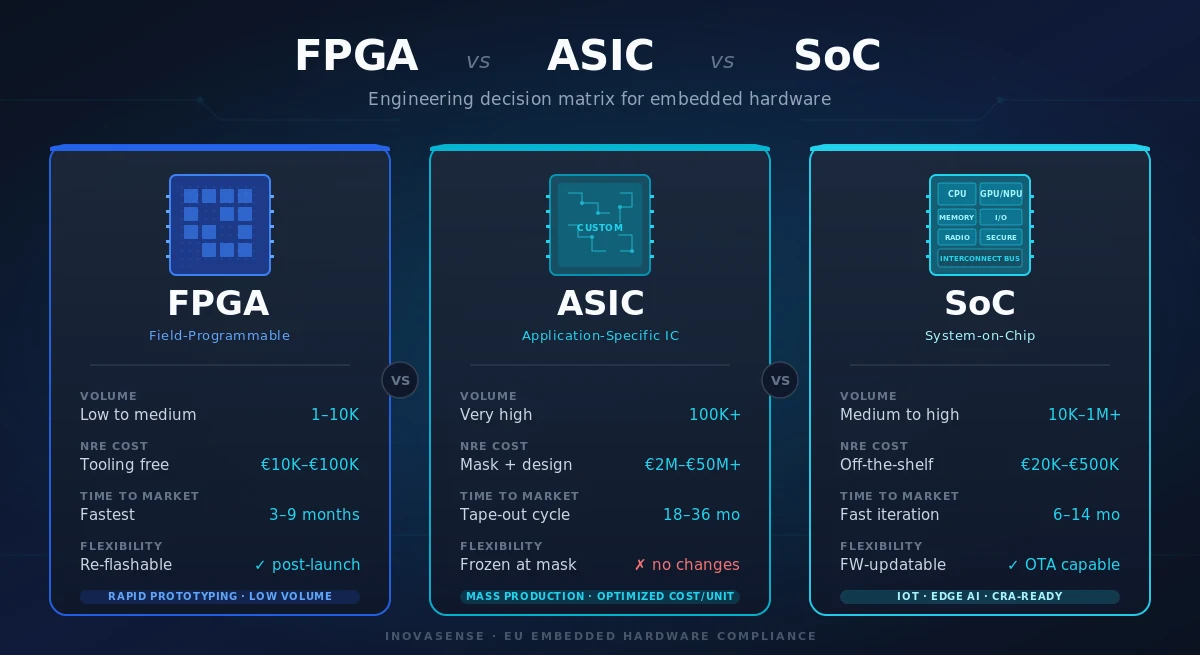
Head-to-Head: FPGA vs ASIC vs SoC
| Criterion | FPGA | ASIC | SoC |
|---|---|---|---|
| Reconfigurability | Full — reprogram in field via JTAG or OTA | Fixed after fabrication | Firmware updatable; silicon fixed |
| Time-to-Market | 3–6 months (RTL to working hardware) | 12–24 months (RTL to first silicon) | Weeks to months (off-the-shelf silicon) |
| NRE Cost | €10K–€150K (RTL + tools + board) | €500K–€10M+ (mask sets + verification + foundry) | €30K–€80K (board + firmware) |
| Unit Cost (10K units) | €15–€200 per chip | €2–€50 per chip (amortized NRE) | €1–€15 per chip (commodity silicon) |
| Clock Frequency | 200–800 MHz typical | 1–5 GHz achievable | 200 MHz – 3.6 GHz depending on SoC class |
| Power Efficiency | 2–10× higher power than equivalent ASIC | Optimized — lowest power per function | Vendor-optimized; varies widely (MCU class to AP class) |
| Logic Density | Up to 9.4M logic elements (Intel Agilex 9) | Virtually unlimited (limited by die area) | Pre-fixed by vendor |
| Security | Bitstream encryption, secure boot, PUF available | Tamper-resistant by design, custom security blocks | TrustZone, Secure Element integration, PSA Certified options |
| IP Protection | Bitstream encryptable but extractable | Mask-level obfuscation — hardest to reverse-engineer | Application code only; silicon IP belongs to vendor |
| CRA Vulnerability Patch Path | Signed bitstream OTA — days to weeks | New mask set required — months to recall | Firmware OTA + vendor patch coordination |
| EU-Sovereign Option | NanoXplore (FR) | EU foundries (X-FAB, GlobalFoundries Dresden) | STMicroelectronics, NXP, Infineon |
For decision-grade specifications and EU-sovereign options across silicon classes, see our FPGA Design Services and EU Hardware Sovereignty capabilities.
When to Choose FPGA
FPGAs are the right choice when one or more of these conditions apply:
1. Your Requirements Will Change
If your product needs post-deployment hardware updates — whether for new protocol support, algorithm improvements, or security patches — FPGA is the only option that doesn’t require a board redesign. This is particularly critical under the EU Cyber Resilience Act, which mandates authenticated firmware updates and vulnerability response throughout a product’s lifecycle (minimum 5 years from market placement).
2. Low-to-Medium Volume Production
For production volumes below 10,000–50,000 units, the NRE savings of FPGA almost always outweigh the higher per-unit cost. The crossover point depends on chip complexity:
| Production Volume | FPGA Total Cost | ASIC Total Cost | Winner |
|---|---|---|---|
| 100 units | €25,000 | €2,500,000+ | FPGA |
| 1,000 units | €60,000 | €2,550,000 | FPGA |
| 10,000 units | €350,000 | €2,700,000 | FPGA |
| 50,000 units | €1,500,000 | €3,000,000 | Depends on complexity |
| 100,000 units | €3,000,000 | €3,500,000 | Breakeven zone |
| 500,000+ units | €15,000,000 | €5,000,000 | ASIC |
Estimates based on mid-range complexity designs. Actual costs vary by technology node and design.
3. Real-Time Signal Processing
FPGAs excel at massively parallel operations — they can process hundreds of data streams simultaneously with deterministic latency. Typical applications:
- Radar and sonar processing — Beamforming, pulse compression, CFAR detection
- Software-defined radio (SDR) — Multi-standard baseband processing
- High-frequency trading — Sub-microsecond market data parsing
- Video processing — 4K/8K encoding, computer vision pipelines
- 5G infrastructure — Massive MIMO, fronthaul processing
4. Defense and Aerospace Applications
Defense and dual-use systems overwhelmingly favor FPGAs for several reasons:
- Long product lifecycles (20–30 years) requiring hardware updates
- Low production volumes (hundreds to low thousands)
- Field-upgradeability for threat response
- ITAR/dual-use compliance — reprogrammable hardware avoids some export control restrictions
- Radiation-tolerant FPGA families available (Microchip RTG4, AMD Versal AI Edge, NanoXplore NG-Ultra)
5. Rapid Prototyping and De-Risking
Even if your end goal is ASIC, prototyping on FPGA first reduces risk dramatically. You can validate your RTL design on real hardware, run system-level tests, and iterate — all before committing to a €500K+ mask set.
When to Choose ASIC
ASICs make sense when the design is stable and volume justifies the investment:
1. High-Volume Consumer Products
Smartphones, smartwatches, Wi-Fi routers, Bluetooth earbuds — any product shipping in hundreds of thousands or millions of units. At these volumes, even a €5 per-unit savings on the chip compounds to millions in margin.
2. Extreme Power Constraints
Battery-powered devices where every milliwatt matters. An ASIC can be optimized at the transistor level to eliminate every unnecessary switching event. Typical power savings vs FPGA: 5–10× lower for equivalent functionality.
3. Maximum Clock Frequency
When you need multi-GHz operation — high-speed SerDes, DDR5 memory controllers, or 5G modem basebands — ASICs on advanced nodes (5nm, 3nm) deliver performance that FPGAs simply cannot match.
4. IP Protection Is Critical
If your competitive advantage is in the silicon itself (a proprietary algorithm, a unique sensor interface), ASIC provides far stronger IP protection. Reverse-engineering an ASIC requires electron microscopy and months of work; extracting an FPGA bitstream, while non-trivial, is comparatively easier.
When to Choose SoC
SoCs are the default modern choice for general-purpose embedded products that need a complete computing platform:
1. Linux-Class Embedded Products
If your product needs an operating system, networking stack, GUI, or AI inference framework — choose an SoC. Hardening a custom FPGA SoC from scratch takes years; commodity SoCs like NXP i.MX, Texas Instruments Sitara, or NVIDIA Jetson ship with mature Linux distributions, BSPs, and tooling.
2. Multi-Protocol Connectivity Out-of-the-Box
Wi-Fi + BLE + cellular + Thread/Matter in one chip is fundamentally an SoC story. Espressif ESP32-C6, Nordic nRF5340, NXP i.MX 8M Plus integrate radios that would otherwise require external modules, EMC re-certification, and significant board space.
3. CRA-Compliant Connected Products at Lower Cost
Modern SoCs increasingly ship with built-in security primitives: ARM TrustZone, secure enclaves, hardware random number generators, eFuses for key storage, and PSA Certified Level 2 or higher silicon. These dramatically simplify EU CRA conformity assessment — vendor-provided evidence covers 40–60 % of the security baseline.
4. General-Purpose Embedded with Some Custom Logic
When you need ~80 % standard SoC functionality and ~20 % custom hardware acceleration, SoC FPGA (covered below) is the answer. Pure FPGA is overkill; pure SoC lacks the custom logic capacity.
The Hybrid Approach: FPGA First, ASIC Later
The most sophisticated hardware teams use a phased approach when targeting high-volume:
Phase 1: FPGA Prototype (3–6 months)
├── Validate RTL design on development board
├── Run real-world tests with actual sensors/interfaces
├── Iterate on architecture without NRE penalties
└── Ship initial low-volume production on FPGA

Phase 2: ASIC Conversion (12–18 months)
├── Freeze RTL design based on FPGA-validated architecture
├── Optimize for target technology node
├── Tape out and fabricate
└── Transition production to ASIC at volume crossover
This approach eliminates the biggest risk in ASIC development: designing the wrong thing. By validating on FPGA first, you ensure the RTL is functionally correct before spending millions on fabrication.
SoC FPGA: When You Want Both
SoC FPGA silicon combines a hard processor system (ARM Cortex-A or RISC-V) with programmable FPGA fabric on one die. This is the architecture of choice for advanced industrial, automotive, and defense systems that need both general-purpose computing and custom hardware acceleration.
| SoC FPGA Family | Vendor | CPU | FPGA Fabric | Best For |
|---|---|---|---|---|
| Zynq UltraScale+ MPSoC | AMD (Xilinx) | Quad ARM Cortex-A53 + Cortex-R5 | UltraScale+ | High-end industrial, automotive, video |
| Versal Adaptive SoC | AMD (Xilinx) | Dual Cortex-A72 + AI Engines | 7nm Versal | Edge AI, 5G, defense radar |
| Agilex SoC | Intel (Altera) | Quad Cortex-A53 (HPS) | Agilex 5/7/9 | Datacenter accel, industrial, 5G |
| PolarFire SoC | Microchip | Quad RISC-V (SiFive U54) | 28nm low-power | Security-critical, IoT gateway, rad-tolerant |
| NG-Ultra | NanoXplore (EU) | Quad Cortex-R52 + dual Cortex-A72 | NG fabric | EU-sovereign space, defense, aerospace |
Why SoC FPGA matters for CRA compliance: the hard CPU side typically inherits PSA Certified or SESIP3 security evidence from the silicon vendor, while the FPGA fabric provides field-reprogrammable security patches for the custom logic. This dual-path remediation is the cleanest CRA architecture for security-critical connected products.
EU CRA Compliance: Architecture-Specific Requirements
The EU Cyber Resilience Act (Regulation 2024/2847) full enforcement starts December 11, 2027, with vulnerability reporting obligations kicking in September 11, 2026. The CRA’s eight essential cybersecurity requirements apply identically regardless of silicon architecture — but how each architecture satisfies them differs significantly.
| CRA Requirement (Annex I) | FPGA Implementation | ASIC Implementation | SoC Implementation |
|---|---|---|---|
| Secure-by-default config | Bitstream contains hardened defaults; no debug ports left open in production | Mask-level hardening of factory defaults | Vendor BSP + manufacturer firmware hardening |
| Authenticated updates | Signed bitstream + signed firmware; FPGA verifies both at boot | Signed firmware only (silicon fixed); typically MCUboot or vendor SBSFU | Signed firmware via MCUboot / vendor mechanism + secure enclave key storage |
| Vulnerability handling (Art. 14) | Field-reprogrammable: bitstream OTA pushes patch in hours-days | Silicon vulnerabilities = no field fix; firmware-layer workarounds only | Firmware OTA path; vendor-coordinated for SoC-level CVE response |
| SBOM | Manufacturer generates; FPGA IP cores require provenance tracking | Manufacturer generates; silicon IP from foundry per agreement | Manufacturer + SoC vendor SBOM components combined |
| Cryptographic confidentiality | Hard crypto blocks in fabric (AES, SHA, custom); PUF for key derivation | Custom silicon blocks; highest tamper resistance | TrustZone + Secure Element + hardware crypto accelerator (vendor-provided) |
| Integrity protection | Bitstream signing + runtime integrity monitors | Mask-level tamper resistance + on-die integrity blocks | Secure boot chain + measured boot + TPM/SE |
| Availability under attack | Hardware watchdog + FPGA hardened fabric | Silicon-level resilience by design | RTOS/Linux with DoS protection + hardware watchdog |
| Identity / authentication | PUF + custom crypto for device identity | eFuse + custom silicon ID block | Secure Element provisioning + vendor identity attestation |
Practical CRA Cost Implication
| Architecture | CRA Compliance Cost (5-year lifecycle) | Why |
|---|---|---|
| FPGA | Lowest at <50K units | Field-reprogrammable = cheapest Art. 14 response; no recall cost |
| SoC (PSA Certified) | Lowest at >100K units | Vendor pre-certification reduces conformity assessment effort by 40–60 % |
| SoC (commodity) | Medium | Firmware patches possible; SoC vendor patch coordination required |
| ASIC | Highest | Silicon-level vulnerabilities = no field fix; recall risk and EOL provisioning costs |
For full Article 14 reporting workflow and conformity assessment options, see our CRA Compliance Checklist and CRA Vulnerability Reporting Guide.
EU Hardware Sovereignty Per Architecture
Under the EU Chips Act (Regulation 2023/1781, €43 billion framework) and the increasing dual-use export-control regime (Delegated Regulation 2025/2003), silicon sovereignty is becoming a real procurement constraint for defense, critical infrastructure, and government-funded projects.
| Architecture | EU-Sovereign Options | Constraints |
|---|---|---|
| FPGA | NanoXplore (FR) — NG-Large, NG-Ultra, NG-Medium; space-grade and defense-grade silicon manufactured under EU supply chain | Lower density and clock vs AMD/Intel; limited tooling ecosystem |
| ASIC fab | GlobalFoundries Dresden (DE) — 22FDX, 12LP+; X-FAB (DE) — automotive and analog mixed-signal; STMicroelectronics Crolles (FR) — embedded NVM | No leading-edge nodes (sub-5nm) in EU; advanced AI ASIC fabbed outside EU |
| SoC | STMicroelectronics (FR/IT) — STM32 family, automotive Stellar; NXP (NL) — i.MX, S32; Infineon (DE) — AURIX, PSoC | Substantial portfolio for industrial / automotive / IoT; smartphone-class application processors remain non-EU |
| EU-sovereign hybrid | NanoXplore NG-Ultra (FPGA + Cortex-R52 + Cortex-A72) | Top choice for EU defense space-grade with Linux-class compute |
For defense and dual-use projects, NanoXplore is currently the most strategically significant — it is the only EU-headquartered FPGA vendor with space-qualified silicon and is aligned with both EU Chips Act objectives and EU dual-use export-control simplification.
2026 FPGA Market Landscape
The FPGA ecosystem has matured significantly:
| Vendor | Key Family | Process Node | Max Logic Elements | AI Acceleration | Notable Feature |
|---|---|---|---|---|---|
| AMD (Xilinx) | Versal AI Edge | 7nm | 1.9M LUTs | 400 AI-Engine tiles | Adaptive SoC with integrated ARM cores |
| Intel (Altera) | Agilex 9 | 7nm (Intel 7) | 9.4M LEs | Integrated AI Tensor Blocks | Highest-density FPGA available |
| Lattice | Avant | 16nm FD-SOI | 500K LUTs | — | Ultra-low power (as low as 15 mW) |
| Microchip | PolarFire | 28nm | 481K LEs | — | Radiation-tolerant, lowest static power mid-range |
| Efinix | Titanium Ti180 | 16nm | 180K LEs | — | RISC-V hard core, lowest cost per LUT |
| NanoXplore (EU) | NG-Large / NG-Ultra | 65nm | 540K LE | — | EU-sovereign space-grade FPGA |
Key trend: The line between FPGA and SoC is disappearing. Modern FPGAs like Versal include ARM Cortex-A72 cores, AI accelerators, and programmable logic on a single die — making them complete platforms, not just programmable logic arrays.
FPGA Design Complexity: What It Actually Takes
A common misconception is that FPGAs are “just programming.” In reality, FPGA development requires deep hardware engineering expertise:
| Task | Tools | Expertise Required |
|---|---|---|
| RTL Design | VHDL or SystemVerilog | Digital logic design, FSM design, pipelining |
| Simulation | ModelSim, Vivado Simulator | Testbench creation, functional verification |
| Synthesis | Vivado, Quartus Prime | Timing closure, resource optimization |
| Place & Route | Vendor tools | Floor planning, timing constraint definition |
| Timing Analysis | Static Timing Analysis (STA) | Setup/hold violations, clock domain crossing |
| Board Design | Altium, KiCad | High-speed PCB layout, power integrity, signal integrity |
| Firmware | C/C++ (for soft/hard processors) | Embedded programming, driver development |
This is why many companies outsource FPGA design to specialized teams. The combined skillset spans digital design, analog electronics, embedded software, and PCB engineering — a rare combination to find in a single team.
Common Mistakes in the FPGA vs ASIC vs SoC Decision
| Mistake | Consequence | Better Approach |
|---|---|---|
| Choosing ASIC for a v1 product with uncertain requirements | €2M+ NRE wasted if requirements change | Prototype on FPGA first, convert to ASIC at v2 |
| Choosing the cheapest FPGA without margin | Design won’t fit after adding features | Select FPGA with ≥30 % resource headroom |
| Ignoring CRA Article 14 patch path in architecture | Post-launch silicon-level vulnerability = recall | Include vulnerability remediation analysis in architecture decision |
| Selecting non-PSA-Certified SoC for connected product | Higher CRA conformity assessment effort and risk | Default to PSA Level 2+ silicon for CRA-scope products |
| Ignoring power budget in FPGA selection | Battery life falls short of spec | Model power consumption early using vendor tools |
| Assuming FPGA = no hardware design | PCB and power delivery fail | Budget for proper high-speed PCB design |
| Skipping timing constraints | Intermittent failures in production | Define all clocks, I/O timing, and multicycle paths |
| Treating SoC vendor as silent CRA partner | Vendor cannot patch issues you don’t report; assumed responsibility gaps | Establish explicit CRA support agreement with SoC vendor before committing |
Quick Decision Framework
Use this sequence:
- Production volume? Below 50K → FPGA shortlist. Above 500K → ASIC shortlist. Between → SoC primary, FPGA where custom logic needed.
- CRA risk class? Important Class II / Critical → Notified Body required; favor architectures with vendor PSA Certified evidence or field-reprogrammable patch capability.
- Functional safety needed? ISO 26262 / IEC 61508 / DO-254 → adds documentation overhead; favor architectures with safety-certified silicon (Microchip PolarFire SoC, STM32 Safety, AMD Versal Functional Safety).
- EU sovereignty mandate? Defense/critical infrastructure → NanoXplore (FPGA) or STM32/NXP (SoC) primary; non-EU silicon only with justification.
- Field-upgradability priority? Yes → FPGA or SoC FPGA. No (consumer fixed-function) → ASIC at volume.
The output should be a shortlist of 2–3 silicon candidates matching your decision path. Final selection should always include hands-on evaluation board work and quoted pricing from at least two vendors.
Related Resources
- CRA Compliance Checklist — Full Cyber Resilience Act requirements for hardware products
- CRA Vulnerability Reporting Guide — Article 14 24-hour reporting workflow
- Dual-Use Export Controls 2026 — How FPGA / ASIC / SoC exports are regulated
- EU Hardware Sovereignty — EU Chips Act and sovereign supply chain
- FPGA Glossary Entry — Quick reference for FPGA terminology
- ASIC Glossary Entry — Quick reference for ASIC terminology
- SoC Glossary Entry — Quick reference for SoC terminology
Our FPGA, ASIC, and SoC Expertise
At Inovasense, silicon architecture decision-making is one of our core services. We work across the full silicon spectrum — from RTL architecture through PCB design to production:
- FPGA design services — AMD Versal, Intel Agilex, Lattice Avant, Microchip PolarFire, and EU-sovereign NanoXplore
- SoC FPGA integration — Zynq UltraScale+, Agilex SoC, PolarFire SoC with full Linux BSP
- FPGA-to-ASIC conversion — phased migration when volume justifies the investment
- Signal processing pipelines — radar, sonar, communications, and Edge AI inference
- Defense and dual-use platforms — rugged designs with security features and EU export-compliance documentation
- EU compliance — CRA, RED, AI Act conformity assessment alongside silicon architecture
Whether you need a complete FPGA-based system, an SoC integration, or an FPGA-to-ASIC migration path, we bring the full hardware development methodology to ensure your design is correct, manufacturable, and certifiable. Contact us to discuss your silicon architecture decision.
Sources & Official References
- Cyber Resilience Act — Regulation (EU) 2024/2847 — EUR-Lex (Official Journal of the EU)
- EU AI Act — Regulation (EU) 2024/1689 — EUR-Lex (Official Journal of the EU)
- EU Dual-Use Regulation — Regulation (EU) 2021/821 — EUR-Lex (Official Journal of the EU)